| CPC H01L 21/76874 (2013.01) [H01L 21/2885 (2013.01); H01L 21/76867 (2013.01); H01L 23/53228 (2013.01); H01L 21/76886 (2013.01)] | 14 Claims |
|
1. A plating method comprising:
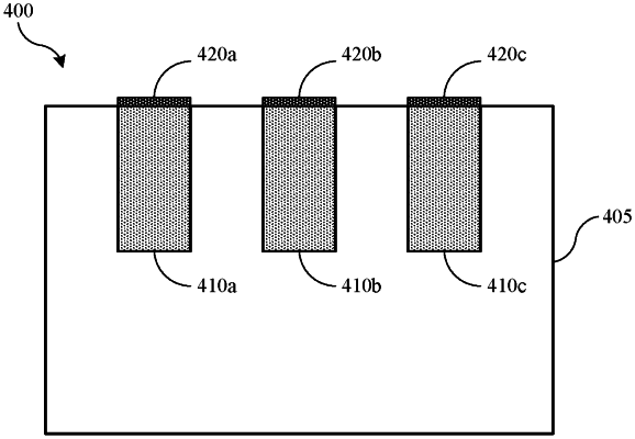
contacting a patterned substrate with a plating bath in a plating chamber, wherein the pattern substrate comprises at least one metal interconnect with a contact surface that is exposed to the plating bath, and wherein the metal interconnect is made of a first metal characterized by a first reduction potential; and
plating a diffusion layer on the contact surface of the metal interconnect, wherein the diffusion layer is made of a second metal characterized by a second reduction potential that is larger than the first reduction potential of the first metal in the at least one metal interconnect,
wherein the plating bath comprises one or more ions of the second metal and a grain refining compound that reduces the formation of pinhole defects in the diffusion layer, the grain refining compound is characterized by a concentration in the plating bath of less than or about 0.05 M, and wherein the diffusion layer is plated on the contact surface of the metal interconnect at a rate of less than or about 5 nm/min.
|