| CPC H01L 21/76829 (2013.01) [H01L 21/7682 (2013.01); H01L 21/76805 (2013.01); H01L 21/76895 (2013.01); H01L 23/535 (2013.01); H01L 23/5329 (2013.01)] | 20 Claims |

|
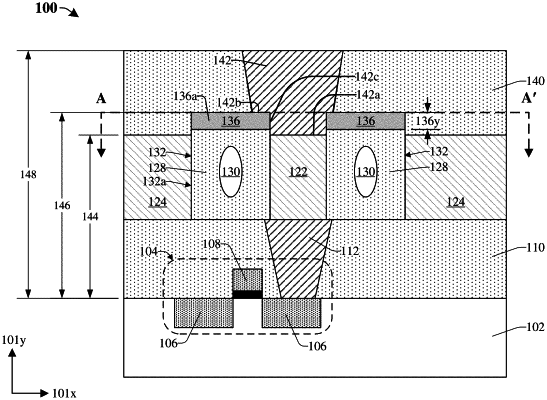
1. A method for forming an integrated chip, the method comprising:
forming a pair of dielectric structures over a substrate and on opposite sides of a first metal line, the pair of dielectric structures comprising a first dielectric;
selectively forming a blocking layer directly over a top surface of the first metal line;
selectively forming a pair of protective etch-stop structures on top surfaces of the pair of dielectric structures, the pair of protective etch-stop structures comprising a second dielectric, different from the first dielectric;
removing the blocking layer from directly over the top surface of the first metal line;
depositing an interlayer dielectric (ILD) layer over the pair of protective etch-stop structures and over the first metal line;
etching the ILD layer to uncover the top surface of the first metal line, wherein the etching is selective to the ILD layer, and wherein the pair of protective etch-stop structures remain on the top surfaces of the pair of dielectric structures throughout the etching; and
forming a metal via directly over the first metal line, wherein the metal via is separated from a first dielectric structure of the pair of dielectric structures by a first protective etch-stop structure of the pair of protective etch-stop structures.
|
|
5. A method for forming an interconnect structure, the method comprising:
depositing a first metal over a substrate;
patterning the first metal to form a first metal line over the substrate and a first opening adjacent to the first metal line;
depositing a first dielectric in the first opening to form a first dielectric structure in the first opening;
forming a blocking layer directly over a top surface of the first metal line;
depositing a second dielectric, different from the first dielectric, on a top surface of the first dielectric structure with the blocking layer in place to form a first protective etch-stop structure on the top surface of the first dielectric structure;
removing the blocking layer from directly over the top surface of the first metal line;
depositing an interlayer dielectric (ILD) layer over the first protective etch-stop structure and over the first metal line;
patterning the ILD layer to form a second opening in the ILD layer directly over the first metal line and directly over the first protective etch-stop structure, wherein patterning the ILD layer comprises etching the ILD layer with high selectivity relative to the first protective etch-stop structure; and
depositing a second metal in the second opening to form a metal via in the second opening directly over the first metal line and directly over the first protective etch-stop structure, wherein the metal via is vertically separated from the first dielectric structure by the first protective etch-stop structure after the second metal is deposited.
|
|
14. A method for forming an integrated chip, the method comprising:
depositing a first metal layer over a substrate;
depositing a hard mask layer over the first metal layer;
patterning the hard mask layer and the first metal layer to form a first metal line over the substrate, a pair of first openings on opposite sides of the first metal line, and a hard mask segment over the first metal line;
depositing a first dielectric layer in the pair of openings, over the first metal line, and over the hard mask segment to form a pair of dielectric structures in the pair of first openings;
forming a blocking layer on the hard mask segment and directly over a top surface of the first metal line;
depositing a second dielectric layer, different from the first dielectric layer, on top surfaces of the pair of dielectric structures with the blocking layer in place to form a pair of protective etch-stop structures on the top surfaces of the pair of dielectric structures;
removing the blocking layer and the hard mask segment from directly over the top surface of the first metal line;
depositing an interlayer dielectric (ILD) layer directly over the pair of protective etch-stop structures and directly over the first metal line;
patterning the ILD layer to form a second opening in the ILD layer directly over the first metal line, wherein patterning the ILD layer comprises etching the ILD layer and the pair of protective etch-stop structures, wherein the etching removes the ILD layer at a faster rate than the pair of protective etch-stop structures; and
depositing a second metal layer in the second opening to form a metal via in the second opening, directly over the first metal line, and over the pair of protective etch-stop structures, wherein the metal via is separated from a first dielectric structure of the pair of dielectric structures by a first protective etch-stop structure of the pair of protective etch-stop structures, and wherein the metal via extends along a sidewall of the first protective etch-stop structure from a top surface of the first protective etch-stop structure to the top surface of the first metal line.
|