| CPC H01L 21/7682 (2013.01) [H01L 21/76826 (2013.01); H01L 21/76828 (2013.01); H01L 21/76831 (2013.01); H01L 21/76832 (2013.01); H01L 29/6656 (2013.01); H01L 29/66795 (2013.01); H01L 29/6653 (2013.01)] | 20 Claims |
|
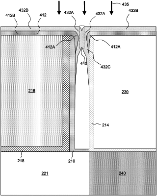
1. A method for forming a semiconductor device, comprising:
forming a first sidewall structure by forming an L-shaped spacer on a sidewall of a gate structure;
forming a second sidewall structure by forming another spacer on a sidewall of a source/drain structure, wherein:
the second sidewall structure is opposite to the first sidewall structure, and
the first and second sidewall structures are formed of different layers and define boundaries of an opening;
depositing a first dielectric material at a first deposition rate on top portions of the opening;
depositing a second dielectric material at a second deposition rate on the first dielectric material and on the first and second sidewall structures, wherein the second dielectric material and the first and second sidewall structures entrap a pocket of air; and
performing a treatment process on the second dielectric material.
|