| CPC H01L 21/6838 (2013.01) [B25B 11/005 (2013.01)] | 20 Claims |
|
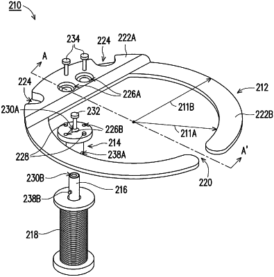
1. A semiconductor manufacturing system, comprising:
a substrate holder;
a substrate displacing assembly for displacing a substrate on the substrate holder in a first direction perpendicular to a top surface of the substrate holder, the substrate displacing assembly comprising:
a pair of load forks, wherein the pair of load forks comprises a fork region and a base region;
a coupler, wherein the coupler comprises a flange region and a tube region, wherein the coupler is mechanically coupled to the base region; and
a driving shaft, wherein the driving shaft is mechanically coupled to the coupler,
wherein a clearance distance in a second direction, perpendicular to the first direction, between an inner wall of the tube region of the coupler to a side wall of the driving shaft is greater than 0.1 millimeters.
|