US 11,901,188 B2
Method for improved critical dimension uniformity in a semiconductor device fabrication process
Chi-Cheng Hung, Toufen Township (TW); Chun-Kuang Chen, Guanxi Township (TW); De-Fang Chen, Hsinchu (TW); Wei-Liang Lin, Hsin-Chu (TW); and Yu-Tien Shen, Hsin-Chu (TW)
Assigned to TAIWAN SEMICONDUCTOR MANUFACTURING COMPANY, LTD., Hsinchu (TW)
Filed by Taiwan Semiconductor Manufacturing Company, Ltd., Hsin-Chu (TW)
Filed on Mar. 28, 2022, as Appl. No. 17/705,615.
Application 17/705,615 is a continuation of application No. 16/925,122, filed on Jul. 9, 2020, granted, now 11,289,338.
Application 16/925,122 is a continuation of application No. 16/042,240, filed on Jul. 23, 2018, granted, now 10,714,357, issued on Jul. 14, 2020.
Application 16/042,240 is a continuation of application No. 15/169,249, filed on May 31, 2016, granted, now 10,032,639, issued on Jul. 24, 2018.
Prior Publication US 2022/0223428 A1, Jul. 14, 2022
This patent is subject to a terminal disclaimer.
Int. Cl. H01L 21/308 (2006.01); H01L 21/027 (2006.01); H01L 21/31 (2006.01); H01L 21/311 (2006.01); H01L 21/033 (2006.01); H01L 21/306 (2006.01); H01L 21/3065 (2006.01); G03F 7/00 (2006.01)
CPC H01L 21/3086 (2013.01) [H01L 21/027 (2013.01); H01L 21/0274 (2013.01); H01L 21/0332 (2013.01); H01L 21/0337 (2013.01); H01L 21/308 (2013.01); H01L 21/3065 (2013.01); H01L 21/3081 (2013.01); H01L 21/3085 (2013.01); H01L 21/3088 (2013.01); H01L 21/30604 (2013.01); H01L 21/31 (2013.01); H01L 21/31144 (2013.01); G03F 7/0035 (2013.01)] 20 Claims
OG exemplary drawing
 
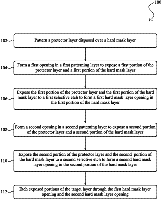
1. A method comprising:
forming a device layer on a substrate;
forming a material layer over the device layer;
forming a protector layer over the material layer;
forming a first patterning layer over the protector layer, wherein a first portion of the protector layer is exposed by the first patterning layer;
removing the first portion of the protector layer;
removing the first patterning layer to expose a second portion of the protector layer;
forming a second patterning layer over the protector layer, wherein the second portion of the protector layer is exposed by the second patterning layer;
removing the second portion of the protector layer; and
patterning the material layer by using the protector layer as a mask, wherein a portion of the device layer is exposed after patterning the material layer.