| CPC H01L 21/3086 (2013.01) [H01L 21/02129 (2013.01); H01L 21/76829 (2013.01); H01L 28/40 (2013.01); H01L 28/60 (2013.01); H01L 29/06 (2013.01)] | 20 Claims |
|
1. A semiconductor device comprising:
a wafer;
an etch stop layer on the wafer;
a lower mold layer on the etch stop layer;
an intermediate supporter layer on the lower mold layer;
an upper mold layer on the intermediate supporter layer;
an upper supporter layer on the upper mold layer; and
a hard mask structure on the upper supporter layer,
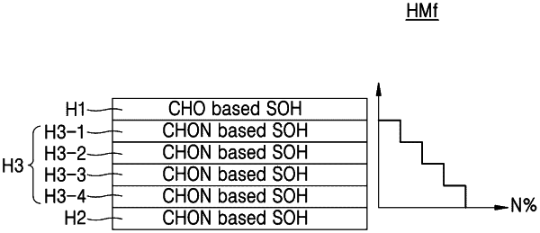
wherein the hard mask structure include a first hard mask layer on the upper supporter layer and a second hard mask layer on the first hard mask layer,
one of the first hard mask layer and the second hard mask layer includes a first organic layer comprising a spin on hard (SOH) mask containing carbon (C), hydrogen (H), oxygen (O), and nitrogen (N), and
the other one of the first hard mask layer and the second hard mask layer includes a second organic layer comprising an SOH containing C, H, and O.
|