| CPC H01L 21/30625 (2013.01) [B24B 37/044 (2013.01); C09G 1/02 (2013.01); H01L 21/0254 (2013.01); H01L 21/02381 (2013.01); H01L 21/02433 (2013.01); H01L 24/83 (2013.01); H01L 2224/83031 (2013.01); H01L 2224/83896 (2013.01)] | 14 Claims |
|
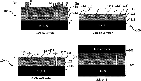
1. A method of reducing surface unevenness of a semiconductor substrate, the semiconductor substrate comprising a deposited layer having surface protrusions resulting from growth imperfections in depositing the deposited layer and a protective layer deposited on the deposited layer, the method comprising:
removing a portion of the deposited layer and the protective layer using a first slurry to reduce the surface protrusions of the deposited layer and to provide an intermediate surface, the first slurry having particles with a hardness level the same as or exceeding that of the deposited layer, wherein the first slurry is adapted to mechanically remove the portion of the deposited layer and the protective layer at a similar removal rate once the surface protrusions are reduced to level with the protective layer to provide the intermediate surface;
depositing a further protective layer on the intermediate surface; and
removing a portion of the further protective layer using a second slurry to reduce surface roughness of the further protective layer and to provide a further intermediate surface,
wherein the deposited layer is a semiconductor layer, and wherein the further protective layer comprises a dielectric layer.
|