| CPC G11C 16/26 (2013.01) [G11C 11/1655 (2013.01); G11C 11/1657 (2013.01); G11C 11/1673 (2013.01); G11C 11/1677 (2013.01); G11C 16/0483 (2013.01); G11C 16/24 (2013.01); G11C 16/3459 (2013.01); H01L 25/0657 (2013.01); H01L 2225/06562 (2013.01)] | 20 Claims |
|
1. A non-volatile memory device, comprising:
a control circuit configured to connect to a plurality of bit lines each connected to one or more non-volatile memory cells, the control circuit comprising:
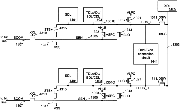
a first sensing circuit including a first sensing node, a first local data bus connectable to the first sensing node, and a first plurality of data latches connected to the first local data bus;
a second sensing circuit including a second sensing node, a second local data bus connectable to the second sensing node, and a second plurality of data latches connected to the second local data bus; and
a connection circuit configured to connect the first local data bus to the second local data bus,
the control circuit configured to:
pre-charge the first sensing node for a first sensing operation of a first selected memory cell along a first bit line;
discharge the pre-charged first sense node through the first selected memory cell by an amount dependent on a programmed state of the first selected memory cell;
based on the amount the first sense node discharged, capacitively store a first sensed value on the first local data bus indicative of the programmed state of the first selected memory cell;
subsequent to capacitively storing the first sensed value on the first local data bus, perform a plurality of logical operations between the first sensed value and values latched in the first plurality of data latches, where to perform the plurality of logical operations the control circuit is configured to:
transfer one or more of the values latched in the first plurality of data latches to the second local data bus over the connection circuit;
perform one or more of the plurality of logical operation using the second plurality of data latches; and
transfer a result of the one or more of the plurality of logical operation using the second plurality of data latches over the connection circuit to the first local data bus; and
concurrently with performing the plurality of logical operations, pre-charge the first sense node for a second sensing operation.
|