| CPC G11C 16/26 (2013.01) [G11C 16/08 (2013.01); G11C 16/10 (2013.01); G11C 16/24 (2013.01); G11C 16/3459 (2013.01); G11C 11/56 (2013.01); G11C 16/0483 (2013.01)] | 19 Claims |
|
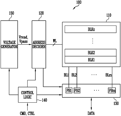
1. A method of operating a semiconductor memory device configured to perform a read operation on selected memory cells, the method comprising:
determining a read voltage to be used in the read operation among first to 2N−1-th read voltages, wherein N is a natural number of 2 or more;
applying a determined read voltage to a selected word line connected to the selected memory cells; and
applying a first read pass voltage or a second read pass voltage greater than the first read pass voltage to adjacent word lines that are adjacent to the selected word line among unselected word lines based on whether the determined read voltage is the first read voltage among the first to 2N−1-th read voltages.
|