| CPC G11C 16/14 (2013.01) [G11C 16/26 (2013.01); G11C 16/30 (2013.01); G11C 16/32 (2013.01)] | 10 Claims |
|
1. A method of operating a memory device, comprising the steps of:
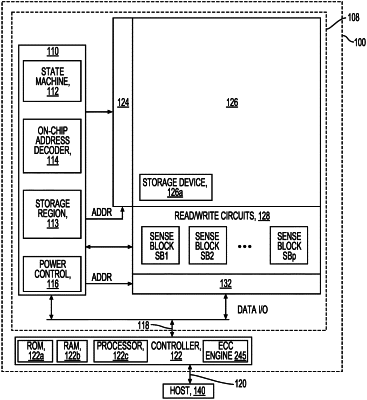
preparing a memory device that includes a plurality of memory cells arranged in an array that includes a plurality of channels that are in electrical communication with a source line; and
in an erase pulse, driving the source line to an elevated voltage that is equal to an erase voltage Vera plus a kick voltage V_kick for a duration t_kick and then reducing the voltage of the source line to the erase voltage Vera to increase channel potential during the entire erase pulse,
wherein the kick voltage V_kick is in the range of 2 and 3 V and the duration t_kick is in the range of 1 and 10 μs.
|