| CPC G09G 3/3677 (2013.01) [G11C 19/28 (2013.01); G09G 2300/0408 (2013.01); G09G 2310/0267 (2013.01); G09G 2310/0286 (2013.01); G09G 2330/021 (2013.01)] | 8 Claims |
|
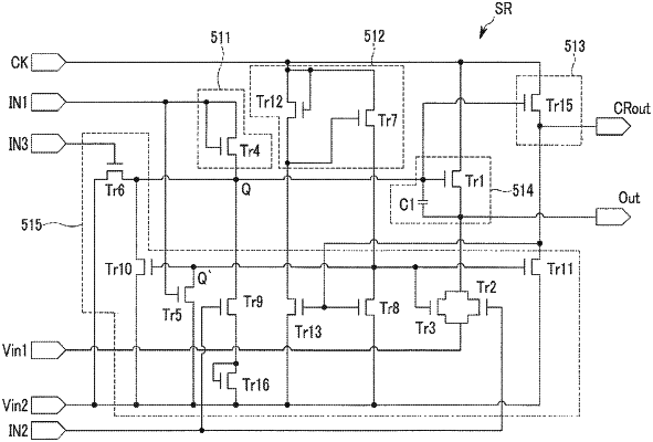
1. A display device comprising:
a display area including a gate line;
a gate driver electrically connected to the gate line, the gate driver including a plurality of stages and being integrated on a substrate,
wherein a stage of the plurality of stages comprises:
a first transistor including a control electrode electrically connected to a first node, a first electrode electrically connected to a clock signal line, and a second electrode electrically connected to the gate line;
a third transistor including a control electrode electrically connected to a second node which is different from the first node, a first electrode electrically connected to a first voff signal line to which a first voff signal is input, and a second electrode electrically connected to the second electrode of the first transistor;
a fifth transistor including a control electrode, a first electrode electrically connected to a second voff signal line, and a second electrode electrically connected to the second node;
an eleventh transistor including a control electrode electrically connected to the second node, a first electrode electrically connected to the second voff signal line, and a second electrode electrically connected to a carry signal out terminal; and
a fifteenth transistor including a control electrode electrically connected to the first node, a first electrode, and a second electrode electrically connected to the carry signal out terminal.
|