| CPC G09G 3/3648 (2013.01) [G02F 1/1368 (2013.01); G02F 1/136286 (2013.01); G09G 2310/08 (2013.01)] | 13 Claims |
|
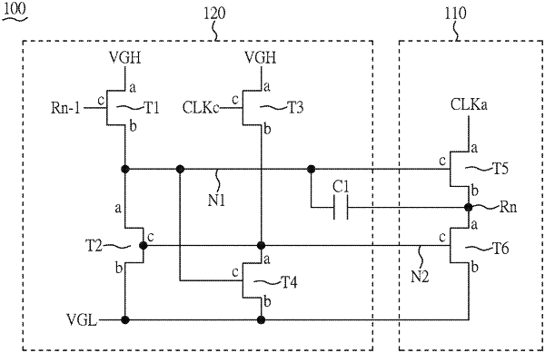
1. A driver circuit, comprising:
an output circuit comprising a pull-up transistor; and
a control circuit coupled to the output circuit, the control circuit comprising a first transistor;
wherein the pull-up transistor has a first control node, and the pull-up transistor is coupled to a first clock signal and a gate line;
wherein the output circuit further comprises an auxiliary transistor coupled to the pull-up transistor and a low voltage, and the auxiliary transistor has a second control node;
wherein the control circuit further comprises a second transistor, a third transistor, a fourth transistor, and a fifth transistor;
wherein a third end of the auxiliary transistor is directly connected to the second transistor, the third transistor, and the fourth transistor;
wherein the first transistor is coupled to a high voltage;
wherein the second transistor is coupled to the low voltage, the first control node, the first transistor, and the fifth transistor;
wherein the third transistor has a first end directly connected to the high voltage, a second end directly connected to the second control node, and a third end directly connected to a second clock signal; and
wherein the fourth transistor is coupled to the low voltage, the first transistor, the fifth transistor, and the auxiliary transistor;
wherein the second transistor has a bottom gate structure, and the auxiliary transistor has a top gate structure.
|