| CPC G09G 3/3291 (2013.01) [G09G 3/3266 (2013.01); G09G 2300/0469 (2013.01); G09G 2360/145 (2013.01); H10K 59/12 (2023.02)] | 7 Claims |
|
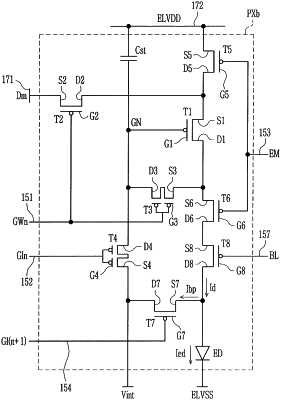
1. A display device, comprising:
a substrate that includes a first surface and a second surface opposing each other, the substrate including a first display area and a second display area that are adjacent to each other;
a scan line disposed on the first surface of the substrate, the scan line for transmitting a scan signal;
a control line for transmitting a control signal that is different from the scan signal;
an emission control signal line for transmitting an emission control signal that is different from the control signal;
a data line and a driving voltage line crossing the scan line and the control line;
a first transistor including a first gate electrode, a first electrode, and a second electrode;
a second transistor including a second gate electrode connected to the scan line, a first electrode connected to the data line, and a second electrode connected to the first electrode of the first transistor;
a light-emitting element including a first electrode and a second electrode;
an optical element disposed below the second surface of the substrate and in the second display area;
a control transistor including a control gate electrode connected to the control line; and
an emission control transistor including an emission control gate electrode connected to the emission control signal line,
wherein
the control transistor, the emission control transistor, and the first transistor are connected to each other in series between the driving voltage line and the first electrode of the light-emitting element.
|