| CPC G09G 3/3266 (2013.01) [G09G 3/3275 (2013.01); G11C 19/28 (2013.01); H01L 27/124 (2013.01); H10K 59/1213 (2023.02); H10K 59/1216 (2023.02); H10K 59/1315 (2023.02); G09G 2300/0842 (2013.01); G09G 2310/0278 (2013.01); G09G 2310/0286 (2013.01); G09G 2310/061 (2013.01); G09G 2320/0233 (2013.01)] | 16 Claims |
|
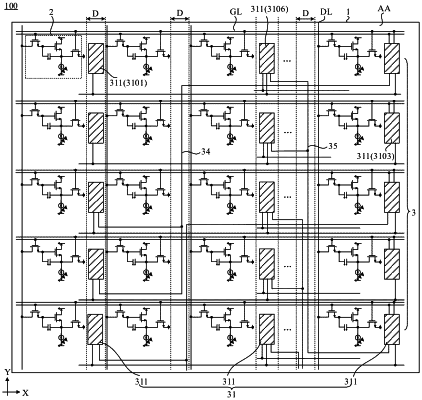
1. The display panel, comprising:
a substrate;
a plurality of sub-pixels on a side of the substrate; the plurality of sub-pixels being arranged in a plurality of rows and a plurality of columns, sub-pixels in a row being arranged in a first direction and sub-pixels in a column being arranged in a second direction; and a sub-pixel including a pixel drive circuit and a light-emitting device electrically connected to the pixel drive circuit;
a gate drive circuit located on a same side of the substrate as the plurality of sub-pixels, wherein the gate drive circuit includes a plurality of cascaded shift registers, and a shift register is electrically connected to a plurality of pixel drive circuits in a row of sub-pixels; the shift register includes a plurality of device groups, and a device group is located in a region between two adjacent sub-pixels in the corresponding row of sub-pixels; and the device group includes at least one transistor and/or at least one capacitor;
a plurality of power supply voltage lines extending along the second direction; and
a plurality of auxiliary power supply voltage lines extending along the first direction, each power supply voltage line being electrically connected to auxiliary power supply voltage lines,
wherein the gate drive circuit further includes a plurality of cascade input signal lines and a plurality of cascade display reset signal lines;
a cascade input signal line is configured to connect a shift signal terminal of one shift register and an input signal terminal of another shift register; a cascade display resit signal line is configured to connect a shift signal terminal of one shift register and a display reset signal terminal of another shift register; and
the display panel has a plurality of sub-pixel regions for arranging the plurality of sub-pixels and first gap regions each located between two adjacent columns of sub-pixels regions; and the cascade display reset signal lines and the cascade input signal lines are disposed in the first gap regions, and both are disposed in different first gap regions;
wherein each sub-pixel region includes a sub-pixel circuit region for arranging a corresponding pixel drive circuit and a sub-pixel light-emitting region for arranging a corresponding light-emitting device that are arranged in the second direction;
in the second direction, any three adjacent rows of sub-pixel regions are a first row of sub-pixel regions, a second row of sub-pixel regions, and a third row of sub-pixel regions; and
a region between the first row of sub-pixel regions and the second row of sub-pixel regions is a second gap region, and a region between the second row of sub-pixel regions and the third row of sub-pixel regions is a third gap region;
wherein in the first row of sub-pixel regions and the second row of sub-pixel regions, sub-pixel light emitting regions are all closer to the second gap region than sub-ixel circuit regions; and
in the second row of sub-pixel regions and the third row of sub-pixel regions, sub-pixel circuit regions are all closer to the thir gap region than sub-pixel light-emitting regions; and
wherein at least three sub-pixel regions constitute a pixel region, each row of pixel regions corresponds to at least one auxiliary power supply voltage line; and
pixel drive circuits in sub-pixels in at least one pixel region corresponding to any auxiliary power supply voltage line are all electrically connected to the auxiliary power supply voltage line.
|