| CPC G09G 3/3266 (2013.01) [G09G 3/3225 (2013.01); G11C 19/28 (2013.01); H10K 59/131 (2023.02); H10K 71/00 (2023.02); G09G 2300/0426 (2013.01); G09G 2310/0281 (2013.01); G09G 2310/0286 (2013.01); G09G 2310/08 (2013.01); G09G 2330/02 (2013.01); H10K 59/1201 (2023.02)] | 12 Claims |

|
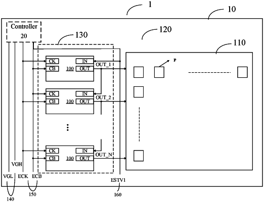
1. A display substrate, comprising:
a base substrate, comprising a pixel array region and a peripheral region; and
a first scan driving circuit, a plurality of power lines, a first signal line group, and a second signal line group, which are in the peripheral region and located on a first side of the base substrate,
wherein the first scan driving circuit comprises a plurality of cascaded first shift registers;
the plurality of power lines are configured to provide a plurality of power voltages to the plurality of cascaded first shift registers in the first scan driving circuit;
the first signal line group comprises at least one timing signal line configured to provide at least one timing signal to the plurality of cascaded first shift registers in the first scan driving circuit;
the second signal line group comprises a first trigger signal line configured to be connected to a first-stage first shift register of the plurality of cascaded first shift registers in the first scan driving circuit and to provide a first trigger signal to the first-stage first shift register; and
the second signal line group is on a side of the plurality of power lines and the first signal line group away from the pixel array region;
the pixel array region comprises a first display region and a second display region, and the first display region and the second display region are juxtaposed to each other and do not overlap with each other, the first scan driving circuit is connected to the first display region to drive the first display region to display,
the display substrate further comprises a second scan driving circuit in the peripheral region and located on the first side of the base substrate, the second scan driving circuit and the first scan driving circuit are sequentially arranged along a scan direction of the pixel array region, and the second scan driving circuit is connected to the second display region to drive the second display region to display,
wherein the second scan driving circuit comprises a plurality of cascaded second shift registers,
the second signal line group further comprises a second trigger signal line configured to be connected to a first-stage second shift register of the plurality of cascaded second shift registers in the second scan driving circuit and to provide a second trigger signal to the first-stage second shift register in the second scan driving circuit;
the first trigger signal line comprises a part extending in an arrangement direction of the plurality of cascaded first shift registers, the second trigger signal line comprises a part extending in the arrangement direction of the plurality of cascaded first shift registers, an extension length of the part of the first trigger signal line and an extension length of the part of the second trigger signal line are identical to length of the first scan driving circuit and length of the second scan driving circuit.
|