| CPC G09G 3/3266 (2013.01) [G09G 3/3291 (2013.01); H10K 59/124 (2023.02); H10K 59/131 (2023.02)] | 11 Claims |
|
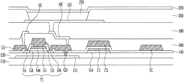
1. A display device, comprising:
a substrate;
a first conductive layer disposed on the substrate;
a first insulation layer disposed on the first conductive layer;
a plurality of active patterns disposed on the first insulation layer, and comprising a source region, a channel region, and a drain region;
a second conductive layer comprising a first gate electrode disposed on the active patterns and that overlaps the channel region, and a driving gate electrode;
a second insulation layer disposed on the second conductive layer; and
a third conductive layer comprising a capacitor electrode and at least one scan line disposed on the second insulation layer,
wherein the capacitor electrode overlaps the driving gate electrode, and the capacitor electrode and the driving gate electrode form a capacitor,
the first conductive layer overlaps the driving gate electrode and the capacitor electrode in orthographic projection, and
all of the active patterns are disposed in a layer located between the substrate and the first gate electrode.
|