| CPC G09G 3/3258 (2013.01) [H10K 59/121 (2023.02); H10K 59/131 (2023.02); G09G 2320/0686 (2013.01)] | 20 Claims |
|
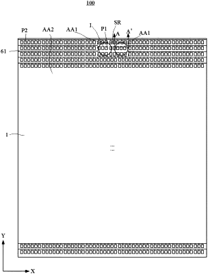
1. A display substrate, comprising:
a first display region and a second display region, wherein a light transmittance of the first display region is greater than a light transmittance of the second display region;
a base substrate;
a plurality of sub-pixels arranged on the base substrate and located in the first display region, wherein the sub-pixels located in the first display region comprise a first pixel driving circuit and a first light-emitting device, and the first pixel driving circuit is electrically connected to the first light-emitting device and configured to drive the first light-emitting device to emit light, and wherein the first pixel driving circuit comprises at least a compensation transistor, a switching transistor, and a light-emitting device initialization transistor, and each of the compensation transistor, the switching transistor and the light-emitting device initialization transistor comprises an active layer;
a plurality of sub-pixels arranged on the base substrate and located in the second display region, wherein the sub-pixels located in the second display region comprise a second pixel driving circuit and a second light-emitting device, and the second pixel driving circuit is electrically connected to the second light-emitting device and configured to drive the second light-emitting device to emit light; and
a scan signal line arranged in the first display region, wherein the scan signal line is configured to provide a scan signal to the first pixel driving circuit,
wherein an orthographic projection of the scan signal line on the base substrate overlaps with an orthographic projection of the active layer of each of the compensation transistor, the switching transistor and the light-emitting device initialization transistor of the first pixel driving circuit on the base substrate.
|