| CPC G09G 3/3233 (2013.01) [G09G 2300/0819 (2013.01); G09G 2300/0842 (2013.01); G09G 2310/0297 (2013.01); G09G 2310/08 (2013.01)] | 20 Claims |
|
1. A display panel, comprising:
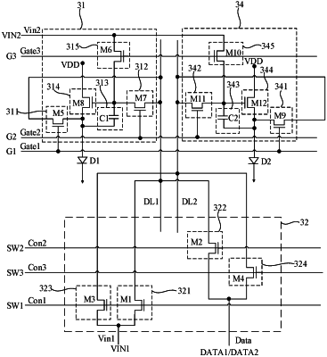
a first pixel circuit, a first multiplexing signal line, and a demultiplexing circuit, wherein
the first pixel circuit comprises a first reset circuit, a first data writing circuit, a first storage circuit, and a first drive circuit, wherein a first terminal of the first reset circuit is connected to a first terminal of the first drive circuit, a second terminal of the first reset circuit is connected to the first multiplexing signal line, the first terminal of the first drive circuit is further connected to a first light-emitting element, a control terminal of the first drive circuit is connected to a first terminal of the first data writing circuit, a second terminal of the first data writing circuit is connected to the first multiplexing signal line, a first terminal of the first storage circuit is connected to the control terminal of the first drive circuit, and a second terminal of the first storage circuit is connected to the first terminal of the first drive circuit; and
the demultiplexing circuit comprises a first control circuit and a second control circuit, wherein a first terminal of the first control circuit is connected to the first multiplexing signal line, a second terminal of the first control circuit is used for receiving a reset signal, a first terminal of the second control circuit is connected to the first multiplexing signal line, and a second terminal of the second control circuit is used for receiving a first data signal;
wherein the display panel further comprises a second pixel circuit and a second multiplexing signal line, wherein the second pixel circuit comprises a second reset circuit, a second data writing circuit, a second storage circuit and a second drive circuit, wherein a first terminal of the second reset circuit is connected to a first terminal of the second drive circuit, a second terminal of the second reset circuit is connected to the second multiplexing signal line, the first terminal of the second drive circuit is further connected to a second light-emitting element, a control terminal of the second drive circuit is connected to a first terminal of the second data writing circuit, a second terminal of the second data writing circuit is connected to the second multiplexing signal line, a first terminal of the second storage circuit is connected to the control terminal of the second drive circuit, and a second terminal of the second storage circuit is connected to the first terminal of the second drive circuit; and
the demultiplexing circuit further comprises a third control circuit and a fourth control circuit, wherein a first terminal of the third control circuit is connected to the second multiplexing signal line, a second terminal of the third control circuit is used for receiving the reset signal, a first terminal of the fourth control circuit is connected to the second multiplexing signal line, and a second terminal of the fourth control circuit is used for receiving a second data signal;
wherein the display panel further comprises a first control signal line, a second control signal line, and a third control signal line, wherein a control terminal of the first control circuit and a control terminal of the third control circuit are respectively connected to the first control signal line, a control terminal of the second control circuit is connected to the second control signal line, and a control terminal of the fourth control circuit is connected to the third control signal line.
|