| CPC G09G 3/32 (2013.01) [G09G 2300/0408 (2013.01); G09G 2300/0443 (2013.01); G09G 2300/0819 (2013.01); G09G 2300/0861 (2013.01); G09G 2310/02 (2013.01); G09G 2310/0286 (2013.01)] | 17 Claims |
|
1. A display device comprising:
a display panel where a plurality of unit pixels are disposed; and
a gate driver disposed on an upper surface of the display panel and integrated in each of the plurality of unit pixels,
wherein each of the plurality of unit pixels is driven independently and comprises a main pixel and a redundancy pixel which emit a same color,
wherein the gate driver supplies a first scan signal and a second scan signal to the main pixel and the redundancy pixel,
wherein an output timing of the first scan signal supplied to the main pixel is same as an output timing of the first scan signal supplied to the redundancy pixel,
wherein an output timing of the second scan signal supplied to the main pixel is different from an output timing of the second scan signal supplied to the redundancy pixel,
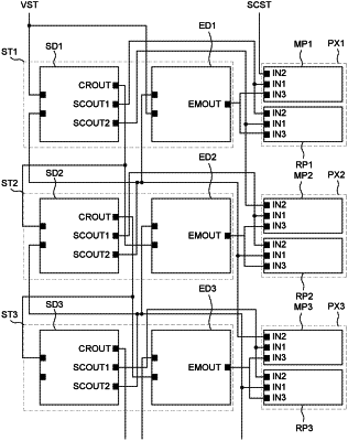
wherein the gate driver comprises a plurality of stages,
wherein an nth stage among the plurality of stages comprises:
a scan driving circuit for outputting the first scan signal, the second scan signal and a carry signal; and
an emission driving circuit for outputting an emission control signal, wherein n is a natural number, and
wherein the scan driving circuit of the nth stage applies the carry signal to a scan driving circuit and an emission driving circuit of an (n+1)th stage, and applies the second scan signal to a scan driving circuit and an emission driving circuit of an (n−1)th stage.
|