| CPC G09G 3/2096 (2013.01) [G06F 3/0412 (2013.01); G06F 3/04166 (2019.05); G06F 3/044 (2013.01); G09G 2310/0289 (2013.01); G09G 2310/06 (2013.01); G09G 2330/021 (2013.01); G09G 2330/028 (2013.01); G09G 2354/00 (2013.01)] | 17 Claims |
|
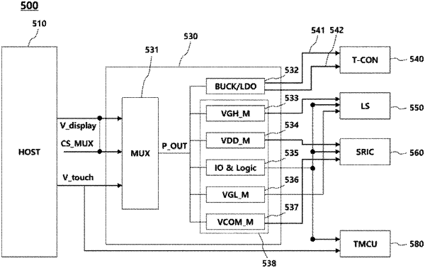
1. A power management integrated circuit comprising:
a multiplexer configured to receive a display voltage or a touch voltage transferred by a host, select one of the display voltage and the touch voltage, and output a multiplexer output voltage;
a buck circuit configured to receive the multiplexer output voltage, reduce a signal level of the multiplexer output voltage, and generate a driving voltage of a timing controller; and
a voltage modulation circuit configured to receive the multiplexer output voltage and generating a gate high voltage, a gate low voltage, a common voltage, and a touch/display driving voltage,
wherein the voltage modulation circuit is configured to modulate and output a waveform of at least one of the gate high voltage, the gate low voltage, the common voltage, and the touch/display driving voltage,
wherein the multiplexer is configured to receive the display voltage as an enable signal to determine an output timing of the multiplexer output voltage.
|