| CPC G09G 3/2096 (2013.01) [G09G 3/32 (2013.01); G09G 3/3275 (2013.01); G09G 2310/0291 (2013.01); G09G 2370/08 (2013.01)] | 4 Claims |
|
1. A display device comprising:
a display panel configured to display an image;
a timing controller configured to control the display panel;
a memory configured to operate in association with the timing controller and disposed on a substrate; and
a data transmission/reception circuit configured to write data into the memory or to read data from the memory under control of the timing controller,
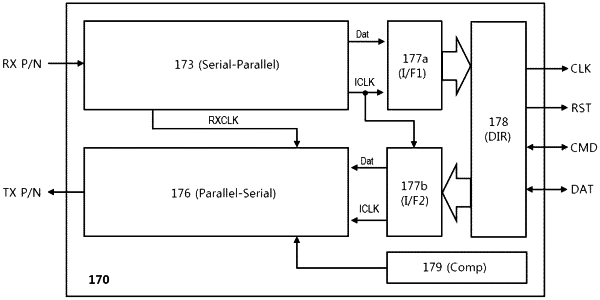
wherein the data transmission/reception circuit includes a transmission direction setting unit configured to set a data transmission/reception path depending on a data transmission period or a data reception period in order to avoid collision between input and output during data transmission/reception,
wherein the data transmission/reception circuit is configured to allow long-range data transmission/reception between the timing controller and the memory, and
wherein the transmission direction setting unit includes a plurality of tri-state buffers and sets the data transmission/reception path according to logic states of enable signals applied to enable terminals of the plurality of tri-state buffers,
wherein the plurality of tri-state buffers includes a data transmission tri-state buffer enabled when data is transmitted, and a data reception tri-state buffer enabled when data is received,
wherein the data transmission/reception circuit includes:
a first interface configured to operate to transmit a data signal transmitted from the timing controller to the memory; and
a second interface configured to operate to transmit a data signal transmitted from the memory to the timing controller,
wherein the enable signal is output from one of the first interface and the second interface, and
wherein the data transmission/reception circuit includes:
a first data format converter configured to receive signals transmitted from the timing controller, to convert a serial data signal from among the signals transmitted from the timing controller into a parallel data signal, and to output the parallel data signal; and
a second data format converter configured to receive signals transmitted from the memory, to convert a parallel data signal from among the signals transmitted from the memory into a serial data signal, and to output the serial data signal.
|