| CPC G06V 40/12 (2022.01) [G06K 19/0718 (2013.01); G06K 19/07354 (2013.01); G06K 19/07747 (2013.01); H01L 23/3121 (2013.01); H01L 2224/16227 (2013.01)] | 20 Claims |
|
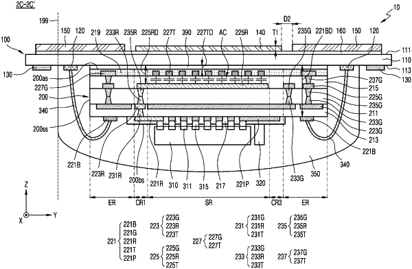
1. A fingerprint sensor package, comprising:
a first substrate including
a core insulating layer including a first surface and a second surface opposite to each other,
a first bonding pad on the second surface of the core insulating layer, and
an external connection pad between an edge of the second surface of the core insulating layer and the first bonding pad;
a second substrate on the second surface of the core insulating layer, the second substrate including
a plurality of first sensing patterns isolated from direct contact with each other in a first direction and extending in a second direction intersecting with the first direction,
a plurality of second sensing patterns isolated from direct contact with each other in the second direction and extending in the first direction, and
a second bonding pad;
a conductive wire electrically connecting the first bonding pad to the second bonding pad;
a controller chip on the second substrate; and
a molding layer on the second surface of the core insulating layer and the second substrate, the molding layer covering the second substrate and the first bonding pad, the molding layer isolated from direct contact with the external connection pad.
|
|
10. A fingerprint sensor package, comprising:
a first substrate including
a core insulating layer including a first surface and a second surface opposite to each other,
a coating layer on the first surface of the core insulating layer,
a ground bezel on the first surface of the core insulating layer, the ground bezel surrounding the coating layer in a first direction and a second direction intersecting with the first direction,
an adhesive layer between the coating layer and the core insulating layer, the adhesive layer further between the core insulating layer and the ground bezel,
a first bonding pad on the second surface of the core insulating layer, and
an external connection pad between an edge of the second surface of the core insulating layer and the first bonding pad;
a second substrate on the second surface of the core insulating layer, the second substrate including
a plurality of first sensing patterns isolated from direct contact with each other in the first direction and extending in the second direction,
a plurality of second sensing patterns isolated from direct contact with each other in the second direction and extending in the first direction, and
a second bonding pad;
a conductive wire electrically connecting the first bonding pad to the second bonding pad;
a controller chip on the second substrate;
connection bumps between the second substrate and the controller chip and electrically connecting the second substrate to the controller chip; and
a molding layer covering the second substrate and the controller chip, the molding layer extending from a side surface of the second substrate to a boundary between the first bonding pad and the external connection pad,
wherein the plurality of first sensing patterns and the plurality of second sensing patterns are isolated from direct contact with each other in a third direction perpendicular to the first and second directions,
wherein the plurality of first sensing patterns and the plurality of second sensing patterns collectively comprise a plurality of capacitors.
|
|
16. A smart card, comprising:
a card main body including a groove region and a connection pad;
a security chip in the card main body; and
a fingerprint sensor package configured to sense a user's fingerprint and transmitting a signal for a sensing result to the security chip,
wherein the fingerprint sensor package includes
a first substrate including
a core insulating layer including a first surface and a second surface opposite to each other,
a first bonding pad on the second surface of the core insulating layer, and
an external connection pad between an edge of the second surface of the core insulating layer and the first bonding pad,
a second substrate on the second surface of the core insulating layer, the second substrate including
a plurality of first sensing patterns isolated from direct contact with each other in a first direction and extending in a second direction intersecting with the first direction,
a plurality of second sensing patterns isolated from direct contact with each other in the second direction and extending in the first direction, and
a second bonding pad,
a conductive wire extending between the first bonding pad and the second bonding pad and electrically connecting the first bonding pad to the second bonding pad,
a controller chip on the second substrate, and
a molding layer on the second surface of the core insulating layer and on the second substrate, the molding layer covering the second substrate and the first bonding pad, the molding layer not covering the external connection pad,
wherein the external connection pad of the first substrate is bonded to the connection pad of the card main body.
|