| CPC G06F 9/30014 (2013.01) [G06F 7/483 (2013.01); G06F 7/5443 (2013.01); G06F 9/30036 (2013.01); G06F 9/30145 (2013.01); G06F 9/382 (2013.01); G06F 9/3802 (2013.01); G06F 9/384 (2013.01); G06F 9/3887 (2013.01); G06N 3/063 (2013.01); G06F 9/30065 (2013.01); G06F 2207/382 (2013.01)] | 18 Claims |

|
1. A processor comprising:
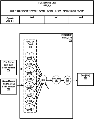
fetch circuitry to fetch a fused multiply-accumulate (FMA) instruction having a plurality of fields usable to identify an opcode, a first input value, a second input value, and a third input value, wherein the first and the second input values each comprise first and second sets of vector data elements, respectively, wherein each of the vector data elements of at least the second set of vector data elements has an M-bit width, wherein the third input value comprises an N-bit accumulation value, where N is an integer multiple of M;
decode circuitry to decode the FMA instruction; and
a single instruction multiple data (SIMD) execution circuit to execute the FMA instruction in an N-bit SIMD lane, the SIMD execution circuit to simultaneously multiply each data element of the second set of vector data elements by a corresponding data element of the first set of vector data elements to produce a plurality of temporary products, and to add the temporary products to the N-bit accumulation value to produce an N-bit result value;
wherein the N-bit SIMD lane is one of a 16-bit lane, a 32-bit lane, and a 64-bit lane, and the M-bit width comprises one of a 4-bit width and an 8-bit width, and
the SIMD execution circuit comprises a first SIMD execution circuit and the N-bit SIMD lane comprises a first N-bit SIMD lane, the processor further comprising a second SIMD execution circuit to execute the FMA instruction in a second N-bit SIMD lane.
|