| CPC G06F 30/398 (2020.01) [G03F 7/705 (2013.01); G03F 7/70441 (2013.01); G06F 30/27 (2020.01); G06F 30/392 (2020.01); G06F 2119/18 (2020.01)] | 20 Claims |
|
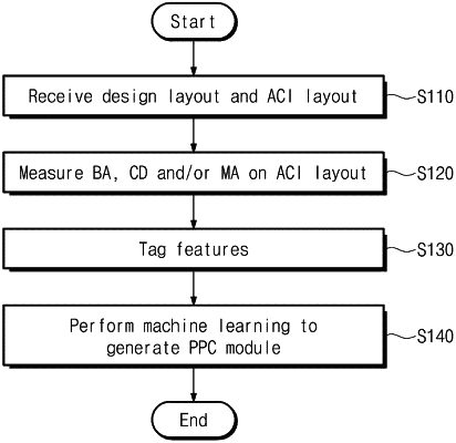
10. An operating method of an electronic device for manufacturing a semiconductor device, the method comprising:
receiving a design layout and an after cleaning inspection (ACI) layout corresponding to the design layout;
measuring at least one of a bias(s), a critical dimension (CD), or a mis-align between the design layout and the after cleaning inspection layout;
tagging features on the after cleaning inspection layout; and
performing learning on a process proximity correction module based on the tagged features and at least one of the bias(s), the critical dimension, or the mis-align.
|