| CPC G06F 3/0653 (2013.01) [G06F 3/0614 (2013.01); G06F 3/0679 (2013.01)] | 20 Claims |
|
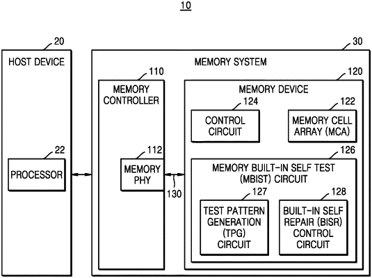
1. A method of testing a memory device including a plurality of memory banks and a memory built-in self-test (MBIST) circuit, wherein the plurality of memory banks include a plurality of memory cells, and the MBIST circuit performs a double data rate (DDR) test or a parallel bit test (PBT), the method comprising:
setting an MBIST option, the MBIST option comprises a DDR test mode and a PBT test mode;
based on the PBT test mode being set as the MBIST option, performing the PBT test on the plurality of memory banks;
based on the DDR test mode being set as the MBIST option, performing the DDR test on one bank selected from among the plurality of memory banks;
based on detecting a defective cell as a result of the DDR test or the PBT test, performing a repair operation for repairing the defective cell with a redundancy cell through the MBIST circuit; and
performing a re-test for verifying the repair operation through the MBIST circuit, wherein the re-test is performed on one or more memory cells including the defective cell among the plurality of memory cells.
|