| CPC G06F 3/04166 (2019.05) [G06F 3/044 (2013.01); G06F 3/04164 (2019.05); H03M 1/18 (2013.01)] | 19 Claims |
|
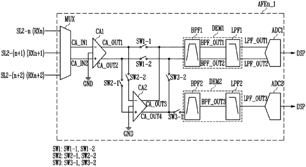
1. An input sensing device, comprising:
electrodes;
a signal processor; and
an analog front-end coupled between the electrodes and the signal processor,
wherein the analog front-end comprises:
a first charge amplifier including input terminals electrically coupled to two electrodes among the electrodes;
a first demodulation circuit electrically coupled to output terminals of the first charge amplifier;
a first analog-to-digital converter coupled to the first demodulation circuit;
a second charge amplifier selectively coupled between the output terminals of the first charge amplifier and input terminals of the first demodulation circuit; and
switching components configured to, in a first mode, couple the output terminals of the first charge amplifier and the first demodulation circuit, and, in a second mode, couple the output terminals of the first charge amplifier and input terminals of the second charge amplifier and couple output terminals of the second charge amplifier and the first demodulation circuit.
|