US 11,899,870 B2
Display device
Shuuichirou Matsumoto, Mobara (JP)
Assigned to Japan Display Inc., Tokyo (JP)
Filed by Japan Display Inc., Tokyo (JP)
Filed on Feb. 21, 2023, as Appl. No. 18/111,977.
Application 18/111,977 is a continuation of application No. 17/565,566, filed on Dec. 30, 2021, granted, now 11,614,817.
Application 17/565,566 is a continuation of application No. 17/101,396, filed on Nov. 23, 2020, granted, now 11,243,631, issued on Feb. 8, 2022.
Application 17/101,396 is a continuation of application No. 16/583,389, filed on Sep. 26, 2019, granted, now 10,877,593, issued on Dec. 29, 2020.
Application 16/583,389 is a continuation of application No. 16/253,379, filed on Jan. 22, 2019, granted, now 10,466,837, issued on Nov. 5, 2019.
Application 16/253,379 is a continuation of application No. 15/831,688, filed on Dec. 5, 2017, granted, now 10,222,905, issued on Mar. 5, 2019.
Application 15/831,688 is a continuation of application No. 15/479,364, filed on Apr. 5, 2017, granted, now 9,864,462, issued on Jan. 9, 2018.
Application 15/479,364 is a continuation of application No. 15/200,925, filed on Jul. 1, 2016, granted, now 9,645,673, issued on May 9, 2017.
Application 15/200,925 is a continuation of application No. 14/702,619, filed on May 1, 2015, granted, now 9,411,466, issued on Aug. 9, 2016.
Application 14/702,619 is a continuation of application No. 13/912,242, filed on Jun. 7, 2013, granted, now 9,052,774, issued on Jun. 9, 2015.
Claims priority of application No. 2012-131154 (JP), filed on Jun. 8, 2012.
Prior Publication US 2023/0205343 A1, Jun. 29, 2023
This patent is subject to a terminal disclaimer.
Int. Cl. G06F 3/041 (2006.01); G06F 3/044 (2006.01); G02F 1/1333 (2006.01); G02F 1/1343 (2006.01); G02F 1/1345 (2006.01); G02F 1/1362 (2006.01); G02F 1/1368 (2006.01)
CPC G06F 3/0412 (2013.01) [G02F 1/1368 (2013.01); G02F 1/13338 (2013.01); G02F 1/13439 (2013.01); G02F 1/13452 (2013.01); G02F 1/134336 (2013.01); G02F 1/136286 (2013.01); G06F 3/044 (2013.01); G06F 3/0416 (2013.01); G06F 3/0445 (2019.05); G06F 3/0446 (2019.05); G06F 3/04166 (2019.05); G02F 1/136295 (2021.01); G02F 2201/121 (2013.01); G02F 2201/123 (2013.01); G06F 2203/04102 (2013.01); G06F 2203/04103 (2013.01)] 4 Claims
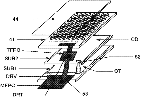
OG exemplary drawing
 
1. A display device comprising:
a first substrate including a plurality of pixel electrodes, a plurality of common electrodes, and a plurality of video lines extending along a first direction;
a display area including the plurality of pixel electrodes and the plurality of common electrodes; and
a chip capable of supplying a common voltage and a touch driving signal to the plurality of common electrodes, and video signals to the plurality of video lines,
wherein
the plurality of common electrodes serve as a counter electrode of the plurality of pixel electrodes and as a touch driving electrode,
the chip has a first long side and a second long side, the first long side and the second long side extending along a second direction,
the chip includes a row of first terminals, each of which is connected to a corresponding one of the plurality of common electrodes, and a row of second terminals, each of which is connected to a corresponding one of the plurality of video lines, and
at least an end of the first long side is closer to the row of the first terminals than the row of second terminals.