| CPC G06F 3/0412 (2013.01) [G06F 3/0446 (2019.05); H10K 50/844 (2023.02); H10K 59/12 (2023.02); H10K 59/38 (2023.02); H10K 59/40 (2023.02); H10K 71/00 (2023.02); G06F 2203/04103 (2013.01); G06F 2203/04111 (2013.01); H10K 59/1201 (2023.02)] | 20 Claims |
|
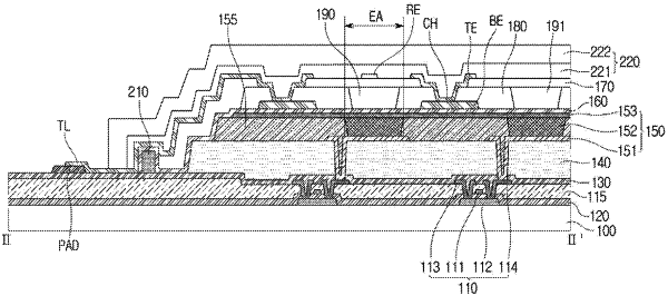
1. An organic light emitting diode display device including a touch sensor, the organic light emitting diode display device comprising:
a substrate having a plurality of light emitting areas defined therein;
a plurality of light emitting elements provided on the plurality of light emitting areas on the substrate;
a first encapsulation film covering the plurality of light emitting elements;
a plurality of color filters provided on the first encapsulation film to respectively correspond to the plurality of light emitting areas;
a plurality of bridge electrodes provided between the plurality of color filters on the first encapsulation film;
a bank insulating film provided on the first encapsulation film to cover the plurality of bridge electrodes and surround the plurality of color filters;
a plurality of touch electrodes provided by being overlapped with the plurality of bridge electrodes on the bank insulating film;
a planarization film covering the plurality of color filters and the bank insulating film and exposing the plurality of touch electrodes; and
a contact penetrating the bank insulating film and connecting a touch electrode and a bridge electrode vertically overlapped with each other among the plurality of touch electrodes and bridge electrodes,
wherein at least one of the plurality of touch electrodes is connected to a touch line provided along a side surface of the planarization film,
wherein the bank insulating film includes a plurality of trenches exposing a portion of an upper surface of the first encapsulation film, corresponding to the plurality of light emitting areas,
wherein the plurality of color filters are disposed in the plurality of trenches,
wherein the plurality of trenches and the plurality of bridge electrodes and the plurality of color filters are disposed on a same plane,
wherein a lowermost surface of each of the plurality of bridge electrodes directly contacts an uppermost surface of the first encapsulation film, a lowermost surface of the bank insulating film directly contacts the uppermost surface of the first encapsulation film, and a lowermost surface of each of the plurality of color filters directly contacts the uppermost surface of the first encapsulation film,
wherein the plurality of bridge electrodes are disposed between the plurality of touch electrodes and the first encapsulation film, each of the plurality of bridge electrodes is disposed under a concave portion of a corresponding touch electrode among the plurality of touch electrodes and directly contacts a lower surface of the concave portion, and a point of contact between the concave portion of the corresponding touch electrode and a corresponding bridge electrode among the plurality of bridge electrodes is disposed in a corresponding trench in the bank insulating film between two adjacent color filters among the plurality of color filters, and
wherein the bridge electrode and the touch electrode vertically overlapped with the bridge electrode and connected to the bridge electrode through the contact do not vertically overlap the plurality of the light emitting areas.
|