| CPC G06F 17/15 (2013.01) [G06F 7/5443 (2013.01); G06F 13/28 (2013.01); G06F 17/14 (2013.01); G06F 17/16 (2013.01); H03H 17/0213 (2013.01)] | 36 Claims |
|
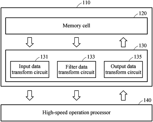
1. A memory device comprising:
a memory configured to store input data and filter data for a convolution operation; and
a function processor, embedded inside the memory device, configured to:
in response to a read command of at least a portion of data from among the input data and the filter data, transform at least a first portion of the input data using a first transforming matrix and transform at least a second portion of the filter data using a second transforming matrix, respectively during a clock cycle corresponding to the read command, the first transforming matrix and the second transforming matrix being respectively based on a parameter of the convolution operation, and output a corresponding transformation result, as transformed data, using a third transforming matrix; and
reduce information loss associated with the outputting by adjusting relationship between the second transforming matrix and the third transforming matrix.
|