| CPC G03F 7/70875 (2013.01) [G03F 7/70633 (2013.01); G03F 7/70891 (2013.01)] | 20 Claims |
|
1. A method, comprising:
receiving a semiconductor workpiece to a process chamber;
forming a photo-sensitive layer on the semiconductor workpiece;
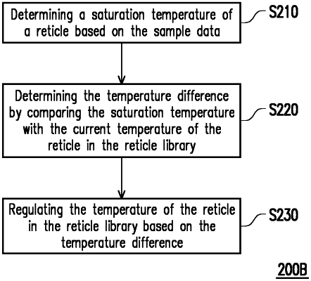
selecting a target state of a reticle based on a given data set, wherein the given data set comprises temperature profiles of the reticle correlated to a target overlay performance, and the target state is a saturation state in which a deformation of the reticle is substantially unchanged;
exposing the semiconductor workpiece by regulating the reticle to reach the target state; and
developing and etching the semiconductor workpiece to form designated patterns on the semiconductor workpiece.
|