| CPC G03F 7/70433 (2013.01) [H01J 37/304 (2013.01); H01J 37/3174 (2013.01); H01J 2237/31769 (2013.01)] | 20 Claims |
|
1. An electron beam lithography system, comprising:
a wafer stage configured to receive a wafer coated with a photo resist;
an electron beam optics to provide an electron beam toward the wafer stage;
a processor; and
a non-transitory memory storing a program,
wherein the program, when executed by the processor, causes the processor to perform:
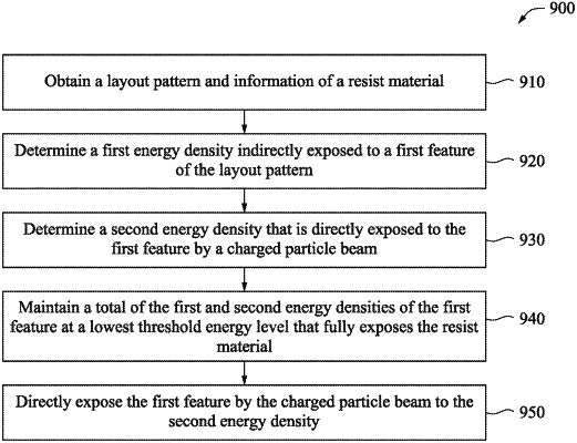
obtaining a layout pattern comprising one or more features to be generated on the photo resist;
obtaining information of the photo resist;
determining a first energy density to a first feature of the one or more features of the layout pattern in the photo resist, based on backscattered electrons when the one or more features of the layout pattern are directly exposed by the electron beam;
determining a second energy density of the first feature when the first feature is directly exposed by the electron beam;
determining a drawing energy density to the first feature based on the first energy density, the second energy density, and the information of the photo resist; and
exposing the first feature of the layout pattern by the electron beam using the drawing energy.
|