US 11,899,368 B2
Manufacturing method of semiconductor device and semiconductor processing system
Yu-Kai Chen, Kaohsiung (TW); Chia-Hung Chung, Tainan (TW); Ko-Bin Kao, Taichung (TW); Su-Yu Yeh, Tainan (TW); Li-Jen Wu, Tainan (TW); Zhi-You Ke, Kaohsiung (TW); and Ming-Hung Lin, Tainan (TW)
Assigned to Taiwan Semiconductor Manufacturing Company, Ltd., Hsinchu (TW)
Filed by Taiwan Semiconductor Manufacturing Company, Ltd., Hsinchu (TW)
Filed on Aug. 9, 2022, as Appl. No. 17/884,519.
Application 17/884,519 is a continuation of application No. 17/372,538, filed on Jul. 12, 2021, granted, now 11,454,891.
Application 17/372,538 is a continuation of application No. 15/905,739, filed on Feb. 26, 2018, granted, now 11,061,333, issued on Jul. 13, 2021.
Claims priority of provisional application 62/584,921, filed on Nov. 13, 2017.
Prior Publication US 2022/0382161 A1, Dec. 1, 2022
Int. Cl. G03F 7/20 (2006.01); G03F 7/40 (2006.01); G03F 7/004 (2006.01); G03F 7/039 (2006.01); G03F 7/16 (2006.01); G03F 7/30 (2006.01); G03F 7/32 (2006.01); H01L 21/027 (2006.01); H01L 21/66 (2006.01); H01L 21/67 (2006.01); H01L 29/66 (2006.01); H01L 29/78 (2006.01)
CPC G03F 7/40 (2013.01) [G03F 7/0046 (2013.01); G03F 7/039 (2013.01); G03F 7/0392 (2013.01); G03F 7/16 (2013.01); G03F 7/20 (2013.01); G03F 7/3092 (2013.01); G03F 7/322 (2013.01); H01L 21/0274 (2013.01); H01L 22/10 (2013.01); H01L 21/67017 (2013.01); H01L 21/67253 (2013.01); H01L 29/66568 (2013.01); H01L 29/78 (2013.01)] 20 Claims
OG exemplary drawing
 
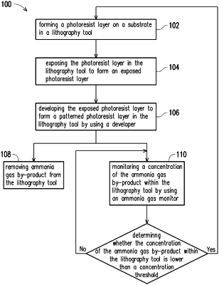
1. A method of manufacturing a semiconductor device, comprising:
developing an exposed photoresist layer using a developer to form a patterned photoresist layer;
discharging an ammonia gas by-product of the developer from a gas outlet of a developer supplying unit; and
disposing an ammonia gas monitor near to the gas outlet of the developer supplying unit.