| CPC G03F 1/32 (2013.01) | 20 Claims |
|
1. A method of manufacturing a mask for use in a semiconductor lithography process performed using light at a lithography wavelength, the method comprising:
providing a substrate coated with a light absorbing layer that is absorbing for the light at the lithography wavelength; and
removing portions of the light absorbing layer to form a mask pattern and a light absorbing border on the substrate;
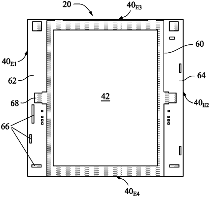
wherein the light absorbing border surrounds the mask pattern, the light absorbing border comprising a portion of the light absorbing layer that is not removed;
wherein the removing includes removing portions of the light absorbing layer on two sides of the light absorbing border to define a peripheral region, the peripheral region including a first peripheral region that extends from an outer perimeter of the light absorbing border to a first edge of the substrate and a second peripheral region that extends from the outer perimeter of the light absorbing border to a second edge of the substrate, the first edge of the substrate and the second edge of the substrate being on opposite sides of the mask pattern; and
wherein the light absorbing border extends to a third edge of the substrate and extends to a fourth edge of the substrate, the third edge of the substrate and the fourth edge of the substrate being on opposite sides of the mask pattern.
|