| CPC G02F 1/2257 (2013.01) [G02F 1/0123 (2013.01); G02F 2202/105 (2013.01)] | 20 Claims |
|
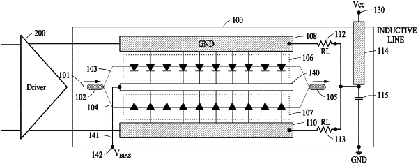
1. A silicon photonics-based optical modulator comprising:
first radio frequency (RF) metal electrodes that operate as grounds;
phase shifters disposed between the first RF metal electrodes and optically modulating optical signals transmitted along optical waveguides;
second RF metal electrodes disposed between the phase shifters, receiving RF electrical signals through one ends thereof from a driving driver located outside of the optical modulator, and providing the RF electrical signals to the phase shifters;
resistor-inductors (RLs) connected at one ends thereof to other ends of the second RF metal electrodes;
an inductive line disposed between a junction point of other ends of the RLs and a power supply for applying a bias voltage to the optical modulator and the driving driver; and
a silicon capacitor disposed between the junction point of the other ends of the RLs and the power supply and preventing a degradation of an RF response characteristic of the optical modulator caused by the inductive line.
|