| CPC G02F 1/167 (2013.01) [G02F 1/1679 (2019.01); G09G 3/20 (2013.01); G09G 2300/0426 (2013.01)] | 14 Claims |

|
1. A display device comprising:
a substrate;
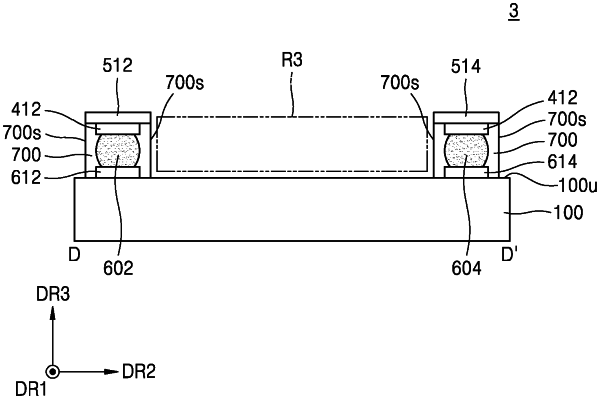
a common electrode layer coupled to the substrate, the common electrode layer comprising a first common pad protruding in a first direction from a first reference side surface extending in a second direction, intersecting the first direction and a second common pad protruding from the first reference side surface;
a driving layer between the substrate and the common electrode layer;
a display layer between the driving layer and the common electrode layer;
a first conductive via apart from the driving layer and between the substrate and the first common pad;
a second conductive via apart from the first conductive via in the second direction;
a driving chip coupled to the substrate and positioned at an opposite side, relative to the driving layer along the first direction, from the first conductive via so that the driving chip and the first conductive via are at opposite sides of the driving layer: and
a protective layer on the common electrode layer, the protective layer comprising a first protective pad on the first common pad and a second protective pad on the second common pad,
wherein the substrate comprises;
a first protruding substrates disposed at the opposite side of the first protective pad with reference to the first conductive via, and
a second protruding substrates disposed at the oposite side of the second protective pad with reference to the second conductive via and protruding from a third reference side surface of the substrate extending in the first direction.
|