| CPC G02F 1/134309 (2013.01) [G02F 1/13439 (2013.01); G02F 1/133514 (2013.01)] | 18 Claims |
|
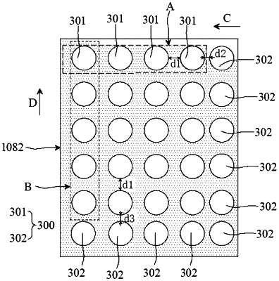
1. An array substrate, comprising: a base substrate, a first electrode, an insulating dielectric layer and a second electrode stacked in sequence; wherein the second electrode is provided with at least one hollow hole, and the hollow hole is in a shape of convex polygon, circle or ellipse;
wherein the hollow hole comprises first hollow holes, and a distance between two adjacent first hollow holes is in a range of 2 μm to 4 μm; and
the hollow hole further comprises a second hollow hole, and the second hollow hole is disposed close to an outer edge of the second electrode; a distance between the second hollow hole and an adjacent first hollow hole is smaller than a distance between two adjacent first hollow holes.
|