US 11,899,319 B2
Thin film transistor substrate including multi-level transparent electrodes having slits
Do-Yeon Kim, Busan (KR); Byung-Sam Min, Goyang-si (KR); and Jong-Hyun Kim, Jeju-si (KR)
Assigned to LG Display Co., Ltd., Seoul (KR)
Filed by LG Display Co., Ltd., Seoul (KR)
Filed on Jul. 15, 2021, as Appl. No. 17/377,172.
Application 17/377,172 is a continuation of application No. 16/517,829, filed on Jul. 22, 2019, granted, now 11,092,857.
Application 16/517,829 is a continuation of application No. 15/373,125, filed on Dec. 8, 2016, granted, now 10,416,502, issued on Sep. 17, 2019.
Claims priority of application No. 10-2015-0177884 (KR), filed on Dec. 14, 2015.
Prior Publication US 2021/0341803 A1, Nov. 4, 2021
Int. Cl. H10K 50/81 (2023.01); H10K 50/82 (2023.01); H10K 50/84 (2023.01); H10K 59/12 (2023.01); H10K 59/13 (2023.01); G02F 1/13 (2006.01); G02F 1/1343 (2006.01); H01L 27/12 (2006.01); G02F 1/1337 (2006.01); G02F 1/1362 (2006.01); G02F 1/1368 (2006.01); G02F 1/1333 (2006.01); H01L 33/44 (2010.01); H01L 33/42 (2010.01); G02F 1/1345 (2006.01); H10K 50/814 (2023.01); H10K 50/824 (2023.01); H10K 50/828 (2023.01); H10K 50/844 (2023.01); H10K 59/123 (2023.01); H10K 59/131 (2023.01)
CPC G02F 1/134309 (2013.01) [G02F 1/1368 (2013.01); G02F 1/13439 (2013.01); G02F 1/133707 (2013.01); G02F 1/134363 (2013.01); G02F 1/136286 (2013.01); H01L 27/1214 (2013.01); G02F 1/1345 (2013.01); G02F 1/133397 (2021.01); G02F 1/134345 (2021.01); G02F 1/134372 (2021.01); G02F 2201/121 (2013.01); G02F 2201/123 (2013.01); G09G 2300/0465 (2013.01); H01L 27/124 (2013.01); H01L 33/42 (2013.01); H01L 33/44 (2013.01); H10K 50/814 (2023.02); H10K 50/824 (2023.02); H10K 50/828 (2023.02); H10K 50/844 (2023.02); H10K 59/123 (2023.02); H10K 59/131 (2023.02); H10K 59/1315 (2023.02)] 6 Claims
OG exemplary drawing
 
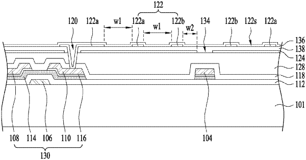
1. A display device having a thin film transistor substrate, the thin film transistor substrate comprising:
a data line;
a transparent upper electrode that is non-overlapping with the data line, the transparent upper electrode including a transparent first electrode, at least two transparent second electrodes and a first slit disposed between the at least two transparent second electrodes, the transparent first electrode closer to the data line than the at least two transparent second electrodes; and
a transparent lower electrode including a second slit that overlaps the data line.