| CPC G02F 1/03 (2013.01) [G02B 6/13 (2013.01); G02F 1/05 (2013.01); G03F 7/70008 (2013.01); G02B 2006/1204 (2013.01); G02B 2006/12045 (2013.01)] | 19 Claims |
|
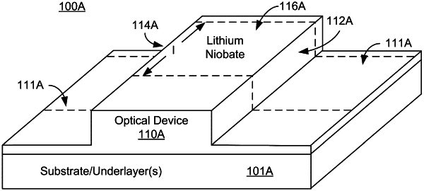
1. A device, comprising:
an optical device, at least a portion of the optical device including at least one ferroelectric nonlinear optical material, the at least the portion of the optical device being fabricated utilizing ultraviolet (UV) photolithography and including a sidewall;
wherein the sidewall is fabricated using the UV photolithography, a first etch and a second etch, the UV photolithography being used to form a mask for fabricating a hard mask from a hard mask layer, the first etch for removing a portion of the hard mask layer to form the hard mask, the second etch for removing a portion of the at least one ferroelectric nonlinear optical material to form the sidewall, the second etch being selected from a dry etch, a reactive ion etch (RIE), a plasma etch and a chemical etch, the second etch being different from the first etch such that the sidewall has a short range root mean square roughness of less than ten nanometers.
|