| CPC G02F 1/0155 (2021.01) [G02F 1/025 (2013.01)] | 14 Claims |
|
1. A method of equalising optical losses, at a required operating wavelength, in waveguide sections in an optoelectronic device comprising a first semiconductor waveguide section and a second semiconductor waveguide section, the method comprising:
determining a first optical loss through the first semiconductor waveguide section for a signal with the required operating wavelength;
determining a second optical loss through the second semiconductor waveguide section for the signal;
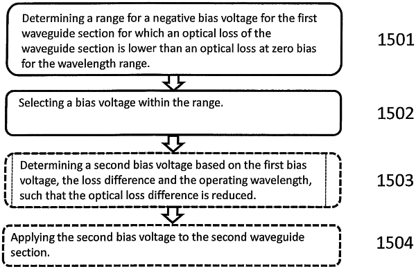
determining a loss difference between the first optical loss and the second optical loss;
determining a first bias voltage based on the loss difference and the required operating wavelength, such that the loss difference and the first optical loss are reduced, wherein determining the first bias voltage comprises:
determining a range of negative bias voltages for which, when a negative bias is applied to the first semiconductor waveguide section, an optical loss in the first semiconductor waveguide section at the required operating wavelength is lower than an optical loss when zero bias is applied to the first semiconductor waveguide section for the required operating wavelength; and
selecting a bias voltage within the range; and
applying the first bias voltage to the first semiconductor waveguide section.
|