| CPC G02B 1/14 (2015.01) [G02B 5/3025 (2013.01); B32B 2307/42 (2013.01); B32B 2457/202 (2013.01); B32B 2457/206 (2013.01); Y10T 156/108 (2015.01); Y10T 156/1082 (2015.01)] | 6 Claims |
|
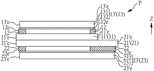
1. An electronic device, comprising:
a panel, comprising:
a first substrate;
a second substrate, disposed opposite to the first substrate;
a first protection element, disposed on a surface of the first substrate away from the second substrate;
a first polarizer, disposed on the first protection element; and
a second protection element, disposed on a surface of the second substrate away from the first substrate,
wherein a width of the first protection element is different from a width of the second protection element.
|