| CPC G01R 33/072 (2013.01) [H10N 52/101 (2023.02); H10N 52/80 (2023.02); H10N 52/01 (2023.02)] | 25 Claims |

|
1. An electronic device, comprising:
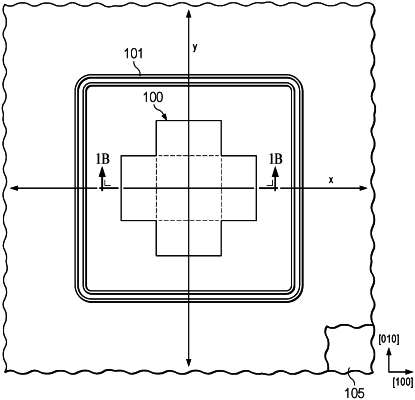
first and second doped regions both having a first conductivity type formed in a semiconductor substrate having a second conductivity type;
a dielectric layer between the first and second doped regions and a surface plane of the semiconductor substrate;
first, second, third and fourth terminals connected to the first doped region, the first and third terminals defining a first conductive path through the first doped region and the second and fourth terminals defining a second conductive path through the first doped region, the second conductive path intersecting the first conductive path;
a first coil formed in an interconnect level over the first doped region, and a second coil formed in the interconnect level over the second doped region;
a well region having the second conductivity type laterally between the first doped region and the semiconductor substrate and bounding a perimeter of the first doped region; and
a control circuit configured to produce a current that when flowing produces:
a first magnetic moment by the first coil, the first magnetic moment having a normal component with a first direction with respect to the surface plane; and
a second magnetic moment by the second coil, the second magnetic moment having a normal component with a second opposite direction with respect to the surface plane.
|