| CPC G01R 31/3177 (2013.01) [G01R 31/2896 (2013.01); G01R 31/31703 (2013.01); G01R 31/318513 (2013.01); G01R 31/318536 (2013.01); G01R 31/318538 (2013.01); G01R 31/318552 (2013.01); G01R 31/318566 (2013.01)] | 20 Claims |
|
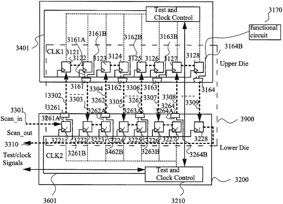
1. A device comprising:
a first die having disposed thereon a first plurality of latches; and
a second die having disposed thereon a second plurality of latches, wherein:
each latch of the first plurality of latches on said first die operatively couple to a respective latch in the second plurality of latches on said second die,
a scan path comprises a closed loop comprising each of said first and second plurality of latches, wherein the scan path goes consecutively through a first latch in the first plurality of latches in the first die, a second latch in the second plurality of latches in the second die, a third latch in the second plurality of latches in the second die, and a fourth latch in the first plurality of latches the first die,
the first latch and the fourth latch are adjacent to each other in the first die, and
the second latch and the third latch are adjacent to each other in the second die.
|