| CPC G01R 31/2815 (2013.01) [G01R 31/2818 (2013.01); G09G 3/006 (2013.01); H05K 1/18 (2013.01); H05K 2201/10128 (2013.01)] | 16 Claims |
|
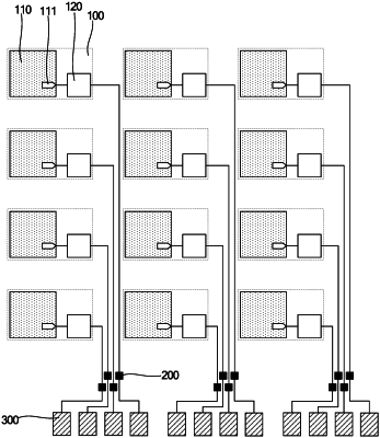
1. A circuit board, comprising a plurality of rows of pixel circuits for progressive scanning, and a plurality of detection terminals, wherein
one pixel circuit of the plurality of rows of pixel circuits comprises a drive unit and a detection unit,
the drive unit comprises a signal output terminal for outputting a drive signal,
the detection unit comprises an input terminal electrically connected to the signal output terminal, and an output terminal electrically connected to one of the plurality of detection terminals,
the detection units in one row of the pixel circuits are electrically connected to different detection terminals,
the detection terminal is electrically connected to an external electrical performance detection circuit, and
wherein the detection unit is configured to electrically connect the signal output terminal to the detection terminal in a process of electrical performance detection and when the drive signal is outputted from the signal output terminal; and disconnect the signal output terminal from the detection terminal in a process other than the electrical performance detection,
wherein the drive unit comprises a first reset module, a data writing module, a light-emission control module, a storage capacitor, and a drive transistor, wherein
the first reset module is configured to connect a control terminal of the drive transistor to a first reset voltage terminal in response to a first control signal;
the data writing module is configured to, in response to a second control signal, connect a first terminal of the drive transistor to a data voltage terminal, and connect the control terminal of the drive transistor to a second terminal of the drive transistor;
the light-emission control module is configured to, in response to a third control signal, connect the first terminal of the drive transistor to a first power supply voltage terminal, and connect the second terminal of the drive transistor to the signal output terminal; and
a first terminal of the storage capacitor is electrically connected to the first power supply voltage terminal, and a second terminal of the storage capacitor is electrically connected to the control terminal of the drive transistor, and the drive transistor is configured to output the drive signal.
|