| CPC B81B 7/007 (2013.01) [B81C 1/00301 (2013.01); B81B 2201/0271 (2013.01); B81B 2203/0127 (2013.01); B81B 2207/012 (2013.01); B81B 2207/07 (2013.01); B81B 2207/097 (2013.01); B81C 2203/0792 (2013.01)] | 20 Claims |
|
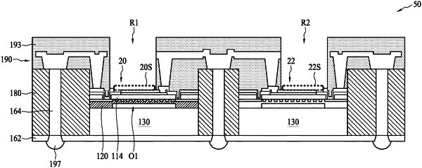
1. A semiconductor device, comprising:
a first device and a second device disposed adjacent to the first device;
a conductive pillar disposed adjacent to the first device or the second device;
a molding surrounding the first device, the second device and the conductive pillar; and
a redistribution layer (RDL) over the first device, the second device, the molding and the conductive pillar, wherein the RDL electrically connects the first device to the second device and includes an opening penetrating the RDL and exposing a sensing area over the first device.
|