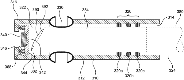
| CPC A61B 1/127 (2013.01) [G02B 1/18 (2015.01); G02B 27/0006 (2013.01); H05H 1/2406 (2013.01); A61L 2/14 (2013.01); A61L 2202/24 (2013.01); H05H 2245/30 (2021.05)] | 15 Claims |

|
1. A device for inhibiting condensation distortion on an optical element, the device comprising:
a housing;
a chamber within the housing, the chamber being configured to accommodate a dielectric barrier at least partially therein;
electrical circuitry in the housing, the electrical circuitry including a plurality of electric conductors;
a plasma activation region associated with the chamber and being configured to retain the optical element in a manner exposing an optical surface of the optical element thereof to the plasma activation region, wherein when the dielectric barrier is at least partially contained within the chamber:
the plasma activation region is configured to contain gas on a first side of the dielectric barrier, and
at least a first electric conductor of the electrical circuitry is configured to form an electrical connection with a first electrode located on the first side of the dielectric barrier;
a second electrode connected to at least a second electric conductor of the electrical circuitry, the second electrode being located on a second side of the dielectric barrier, opposite the plasma activation region, when the dielectric barrier is at least partially contained within the chamber; and
at least one processor configured to:
control electricity flow through the circuitry to cause an electric field associated with a voltage drop between the first electrode located on the first side of the dielectric barrier and the second electrode located on the second side of the dielectric barrier, to thereby generate plasma within the plasma activation region; and
maintain the generated plasma in the plasma activation region for a time period sufficient to cause the optical surface of the optical element to become hydrophilic.
|