| CPC G09G 3/3266 (2013.01) [G09G 3/3258 (2013.01); G11C 19/28 (2013.01); G11C 19/287 (2013.01); G09G 2310/0286 (2013.01); G09G 2310/08 (2013.01)] | 19 Claims |
|
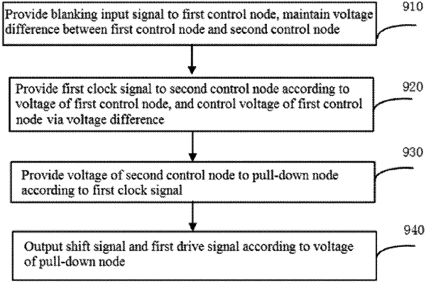
1. A shift register comprising a blanking input circuit, a blanking control circuit, a blanking pull-down circuit, and a shift register circuit;
wherein the blanking input circuit is configured to provide a blanking input signal from a blanking input signal terminal to a first control
wherein the blanking control circuit
wherein the blanking pull-down circuit is configured to provide a voltage of the second control node to a pull-down node according to
wherein the shift register circuit is configured to provide a shift signal via a shift signal output terminal and a first drive signal via a first drive signal output terminal according to a voltage of the pull-down node [ ; and
wherein the shift register circuit further comprises a twenty-ninth transistor, wherein a control electrode of the twenty-ninth transistor is coupled to the pull-down node, a first electrode of the twenty-ninth transistor is coupled to a first voltage terminal, and a second electrode of the twenty-ninth transistor is coupled to the second electrode of the third transistor] .
|