| CPC H10K 50/844 (2023.02) [H10K 59/38 (2023.02); H10K 71/00 (2023.02)] | 20 Claims |
|
1. A display substrate, comprising:
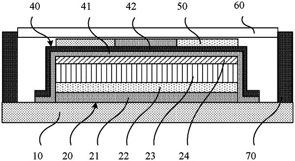
a base substrate, a light-emitting element disposed on the base substrate, and an encapsulation layer disposed on the light-emitting element, wherein:
the display substrate further comprises a driving circuit connected with the light-emitting element and configured to drive the light-emitting element, the driving circuit comprises a driving transistor which comprises an active layer located inside the base substrate;
the encapsulation layer comprises a first gradient layer and a second gradient layer stacked along a direction away from the base substrate;
in a direction perpendicular to the base substrate and from a layer where the base substrate is located to a layer where an uppermost layer of the display substrate is located, a content of oxygen element in the first gradient layer of the encapsulation layer gradually decreases;
in the direction perpendicular to the base substrate and from the layer where the base substrate is located to the layer where the uppermost layer of the display substrate is located, a content of carbon element in the second gradient layer of the encapsulation layer gradually increases; and
the encapsulation layer comprising the first gradient layer and the second gradient layer is formed with a structure of material functional gradient change.
|