| CPC H05K 5/0217 (2013.01) [H01R 12/7023 (2013.01); H01R 12/721 (2013.01); H01R 12/73 (2013.01); H01R 13/621 (2013.01); H05K 5/0008 (2013.01); H05K 5/026 (2013.01); H05K 7/20409 (2013.01); H01L 25/18 (2013.01); H05K 1/117 (2013.01); H05K 1/181 (2013.01); H05K 7/20445 (2013.01); H05K 2201/09063 (2013.01); H05K 2201/10159 (2013.01)] | 13 Claims |
|
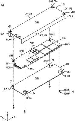
1. A memory device comprising:
an enclosure assembly comprising a first enclosure located at the top and a second enclosure located at the bottom; and
a memory module disposed within the enclosure assembly,
wherein the memory module comprises a module board configured with a plurality of non-volatile memory chips, a memory controller, a memory connector, and a plurality of module fastening holes,
wherein the memory connector protrudes outward in a first direction from a first short side of the module board,
wherein the first enclosure comprises a first main cover that covers upper faces of the module board and the second enclosure comprises a second main cover which at least partially covers a lower face of the module board,
wherein at least one clamping hole penetrates the first main cover at a position overlapping the memory connector, and has a space for a hook of a host connector when the memory device is connected to a host device,
wherein the first enclosure comprises only three inter-device fastening pillars, each including a fixed hole extending through the inter-device fastening pillar and the first main cover, and
wherein ends of the fixed holes are open at the end portions of the inter-device fastening pillars and opposite ends of the fixed holes are open on an upper face of the first main cover.
|