|
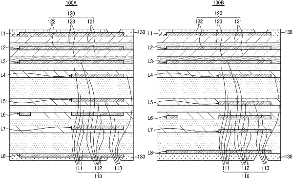
6. A printed circuit board comprising: a first substrate portion including a plurality of first insulating layers, a plurality of first wiring layers respectively disposed on the plurality of first insulating layers, and a plurality of first adhesive layers respectively disposed between the plurality of first insulating layers to respectively cover the plurality of first wiring layers; and a second substrate portion disposed on the first substrate portion, and including a plurality of second insulating layers, and a plurality of second wiring layers respectively disposed on the plurality of second insulating layers, wherein a dissipation factor of each insulating layer of the plurality of first insulating layers disposed in a region of the printed circuit board at one side of an interface of the first substrate portion and the second substrate portion is lower than a dissipation factor of each insulating layer of the plurality of second insulating layers disposed in another region of the printed circuit board at another side of the interface of the first substrate portion and the second substrate portion; at least one first wiring layer among the plurality of first wiring layers comprises a signal pattern, and at least one other first wiring layer among the plurality of first wiring layers comprises a ground pattern, wherein the at least one other first wiring layer including the ground pattern is disposed on a different level from the at least one first wiring layer including the signal pattern, and wherein the at least one other first wiring layer including the ground pattern is disposed on both sides of the at least one first wiring layer including the signal pattern.
|