| CPC H01L 31/0508 (2013.01) [H01L 31/1876 (2013.01)] | 14 Claims |
|
1. Method of manufacturing a single-side-contacted photovoltaic device, comprising the steps of:
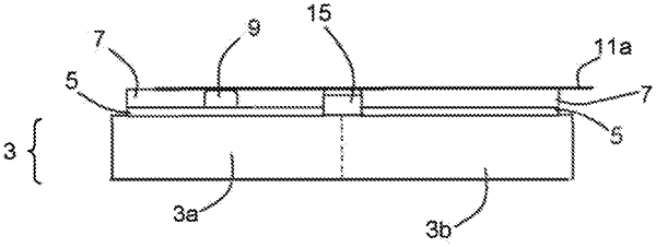
a) providing a photovoltaically-active substrate defining a plurality of alternating hole collecting zones and electron collecting zones arranged in parallel strips;
b) depositing a conductive layer across said zones;
c) depositing at least one conductive track extending along at least part of each of said zones;
d) subsequently to step c), selectively forming a dielectric layer on each of said zones, so as to leave an exposed area free of dielectric at an interface between adjacent zones, in which said selectively-formed dielectric layer remains in the finished photovoltaic device;
e) etching said conductive layer in said exposed areas;
f) applying a plurality of interconnecting conductors so as to electrically interconnect at least a portion of said hole collecting zones with each other, and to electrically interconnect at least a portion of said electron collecting zones with each other.
|